CMOS photo sensor: Complete specifications guide
The CMOS photo sensor plays a central role in the digital transformation of photography. It converts light into electrical signals, enabling the creation of digital images. Widely adopted, CMOS technology offers excellent value for money and outstanding performance.
CMOS sensors are made up of millions of photosites, each corresponding to a pixel in the final image. These photosites use photodiodes to convert light into electrical charge, directly influencing the quality of the captured image. To reproduce colors, these sensors incorporate color filters, such as the famous Bayer filter.
Technological advances have enabled the development of higher-performance CMOS sensors. BSI (Back Side Illumination) versions improve sensitivity by placing the photodiodes on the surface. Stacked CMOS sensors integrate electronic circuits beneath the photodiodes, optimizing light capture and enabling higher reading speeds.
Noise management is crucial to image quality. CMOS sensors employ techniques such as correlated double sampling (CDS) to reduce interference. The type of shutter, rolling or global, influences the capture of moving subjects, an important aspect for many photographers.
Key points to remember
- CMOS sensors transform light into electrical signals
- Each photosite corresponds to one pixel of the final image
- Color filters enable color reproduction
- BSI technology enhances sensor sensitivity
- Stacked sensors deliver better performance
- Noise reduction is essential for image quality
- Shutter type affects capture of moving subjects
Introduction to CMOS photo sensors
CMOS photo sensors mark a crucial step in the evolution of digital photography. They transform light into electrical signals, enabling the creation of high-quality digital images. This technology is fundamental to the production of precise, detailed images.
Definition and basic principles
A CMOS digital image sensor is made up of thousands of photodetectors, called photosites. Each photosite captures light and converts it into electrical current. This technology offers remarkable efficiency, with a high saturation capacity. It allows longer exposures and better image quality.
Historical development of the technology
CMOS sensors have undergone a spectacular evolution since their inception. Initially limited in terms of performance, they have progressed to offer..:
- Lower noise levels
- Higher dynamic range
- Faster reading speeds
Today, models such as Sony Pregius or onsemi PYTHON achieve impressive performance. They go up to 65 megapixels and 1622 frames per second.
Importance in modern digital photography
CMOS sensors have become essential in modern digital photography. Their high quantum efficiency ensures better photon capture. Their compliance with EMVA 1288 standards guarantees objective characterization. These advances have revolutionized image capture, giving photographers ever more powerful tools with which to express their creativity.
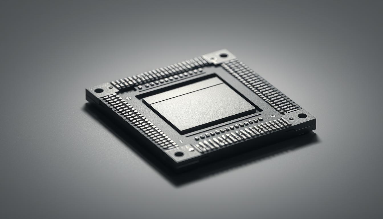
The basic structure of a CMOS photo sensor
The CMOS photo sensor is at the heart of today's digital cameras. It is made up of a dense network of photoreceptor cells, or photodiodes. These crucial elements transform light into the electrical signals essential for image capture.
Each photodiode is linked to a tiny integrated circuit. This circuit contains three transistors: one for reset, one for amplification and one for selection. This organization ensures fast readout and optimum energy efficiency.
MOS (Metal Oxide Semiconductor) technology lies at the heart of the CMOS sensor. When light strikes the semiconductor, electron-hole pairs are created. Electrons travel to the semiconductor-oxide interface, where they are stored in potential wells. They are then transferred to the electronic part for reading.
A Bayer filter covers the photodiodes, with filters for red, green and blue. This arrangement enables color capture. The fill factor of CMOS sensors varies between 30 and 50%, lower than that of CCD sensors. However, CMOS offers superior readout speed and reduced power consumption.
Manufacturing technologies and architectures
CMOS technology has transformed digital photography through continuous innovation. Advances in the photosensitive matrix of CMOS sensors have improved image quality and performance. These advances are essential to the photographic industry.
Traditional CMOS
The traditional CMOS sensor combines a photodiode, transistors and readout circuits in each photosite. This structure reduces energy consumption and production costs. It is more economical than CCD sensors.
CMOS BSI (Back-Side Illuminated)
BSI technology marks a milestone. The sensor is inverted, with the photodiodes facing the light. This arrangement reduces light loss and increases sensitivity.
Stacked CMOS
Stacked CMOS takes things a step further. The sensor is integrated into a microchip, separating the signal readout from the photodiodes. This organization enables the use of larger photodiodes, improving image quality.
These innovations have made it possible to reduce pixel size while increasing resolution. For example, Sony's 4th-generation Pregius sensors have reduced pixel size from 3.45 µm to 2.74 µm. Canon has even created a 250 MP sensor with 1.5 µm pixels. These advances are crucial for the photography industry.
Principle of photosite operation
The heart of modern photography lies in the digital image sensor. It functions thanks to essential components called photosites. These are responsible for converting light into an electrical signal.
Photodiodes and photoelectric conversion
Photodiodes are the central element of photosites. They convert light into electric current. The intensity of this current varies according to the amount of light received. Each photosite is equipped with a color filter, enabling the reproduction of the scene's colors.
Role of transistors
Transistors are crucial to photosite operation. They amplify the electrical signal from the photodiodes, preparing it for reading. This step is vital for obtaining high-quality images, especially in low light conditions.
Signal reading process
The signal is read out sequentially. Each photosite has its own voltage charge converter and amplifier. This architecture ensures fast, accurate reading of the light information captured. Modern CMOS sensors use microlenses to improve quantum efficiency, optimizing light capture.
CMOS photo sensor features and performance
CMOS sensors are distinguished by their outstanding performance in digital photography. Their high image resolution and enhanced light sensitivity make them essential components of modern cameras.
The image resolution of CMOS sensors has improved considerably over the years. Smaller and smaller pixels mean more detailed images. However, pixel size remains a crucial factor. Pixels of 1.4μm or more offer better light capture, improving image quality in low-light conditions.
The light sensitivity of CMOS sensors has taken a quantum leap thanks to BSI (Back-Side Illuminated) technology. This innovation places the circuits behind the photosites, increasing light capture efficiency compared with FSI (Front-Side Illuminated) sensors. Octagonal photosensitive surfaces and micro-lenses further optimize light gathering.
CMOS sensors outperform CCDs in terms of power consumption and processing speed. Each CMOS pixel has its own analog-to-digital conversion circuit, enabling more efficient data management. This architecture facilitates noise reduction and dynamic range enhancement, essential for high-quality images.
Sensitivity and noise management
Managing light sensitivity and noise is essential for capturing high-quality images with a CMOS sensor. These two aspects are interconnected, directly influencing color rendition and photo sharpness.
Electronic noise sources
Several sources contribute to electronic noise in CMOS sensors:
- Shot noise
- Playback noise
- Thermal noise
- Dark current noise
Noise reduction techniques
Manufacturers use various strategies to improve light sensitivity and reduce noise:
- Increased exposure time
- Correlated double sampling
- Sensor cooling
- Black image subtraction
Impact on image quality
Pixel size is crucial to light capture. Larger pixels improve light sensitivity and reduce noise, especially in low-light conditions. Advanced technologies such as backside illumination (BSI) and stacked CMOS sensors optimize light capture and reduce noise, improving color rendering.
However, these advances pose challenges. Increasing pixel size can compromise resolution. BSI technology can introduce more noise and complicate manufacturing. The challenge lies in finding the optimum balance between light sensitivity, noise reduction and overall image quality.
Filter systems and color reproduction
CMOS sensors employ complex filtering systems to ensure accurate color rendition. The photosensitive surface is covered with a Bayer filter, alternating between red, green and blue. This arrangement captures the color information crucial to reconstructing a complete image.
The Bayer filter consists of 2x2 pixel patterns, with two greens, one red and one blue. This organization is based on the sensitivity of the human eye, which is more sensitive to green. Each photosite captures only one primary color, requiring digital processing to obtain the final image.
The dematrixing process estimates the missing color components for each pixel. This essential step determines the quality of color rendering. Advanced methods such as spatial interpolation and frequency techniques are used to reduce artifacts such as aliasing and color smearing.
Innovations such as Sony's BSI sensors improve light capture and reduce noise, enhancing color accuracy. Foveon technology, employed by Sigma, takes a unique approach with superimposed color filters, offering color reproduction without interpolation.
Shutter technology and playback speed
CMOS photo sensors have transformed digital photography. They introduce advanced shutter technologies. These innovations have a direct impact on image quality and camera performance.
Mechanical vs. electronic shutters
Mechanical shutters use physical curtains to regulate exposure. Conversely, electronic shuttering on the digital image sensor activates and deactivates pixels. This method allows faster shutter speeds and reduces vibrations.
Rolling shutter and its effects
The rolling shutter, common in CMOS photo sensors, exposes the image line by line. This technique can distort fast-moving objects. This is particularly true of high-resolution sensors.
Global shutter and applications
The global shutter exposes all pixels simultaneously, avoiding distortion. The Sony A9 III, released in November 2023, is the first consumer camera to adopt this technology. It reaches a maximum shutter speed of 1/80,000s, ideal for high-speed photography without motion blur.
Stacked CMOS sensors, like Sony's Exmor RS, deliver impressive performance. They can read the entire sensor up to 90 times per second, enabling ultra-fast bursts in full definition. Some specialized CMOS cameras even achieve 25,000 frames per second in megapixel resolution.
Recent technological advances
CMOS technology is making significant progress in the field of digital image sensors. Manufacturers are working on higher-performance sensors. They are aiming for better image quality and advanced functionalities.
The integration of artificial intelligence into CMOS sensors opens up new perspectives. Researchers have created a three-layer CMOS image sensor with integrated AI. This sensor is capable of semantic segmentation and object detection. This breakthrough promises revolutionary applications in photography and video.
Advances in miniaturization enable the creation of flexible, foldable sensors. These sensors are ideal for wearable technologies and foldable smartphones. Sensor resolution is improving, with 4K and 8K models offering exceptional video quality for real-time applications.
The automotive and surveillance industries are massively adopting these high-definition sensors. They improve safety and surveillance. CMOS sensors are also finding their way into drones. They offer high-resolution imaging capabilities in a compact format.
These technological advances are propelling the CMOS sensor market forward. The IoT sector is expected to grow by 15% by 2022. Industry giants such as Sony and Samsung continue to innovate. They offer ever more efficient and energy-saving sensors.
Industrial and professional applications
CMOS technology has established itself in many industrial and professional sectors. CMOS photo sensors offer outstanding performance for a wide range of specialized applications.
Wide range of applications
CMOS sensors are ubiquitous in industry. They are used in automotive safety systems, medical imaging and surveillance cameras. Robotics and logistics also benefit from this technology for process automation.
Essential selection criteria
The choice of a CMOS photo sensor depends on the intended application. For professional photography, high resolution is essential. For machine vision systems, acquisition speed and low-light sensitivity are paramount. Pixel size and compatibility with optics are also key factors.
Custom solutions
Companies like Syscom-Prorep offer CMOS solutions tailored to specific requirements. For example, some sensors offer 3.2 effective megapixels with a pixel size of 2.25 µm. They support high acquisition speeds and incorporate advanced features such as fast auto-exposure and quad HDR.
3D imaging and SWIR sensors are booming in the fields of gaming, healthcare and defense. CMOS technology continues to evolve to meet the growing demands of industry and professionals.
Impact on final image quality
The CMOS sensor is essential for image quality. Its resolution determines the sharpness and detail captured. Today's low-light sensors improve photo quality in difficult conditions.
Color filters on the sensor influence color rendering. The common Bayer filter ensures faithful color reproduction. Fujifilm, for example, offers alternatives to reduce moiré.
BSI (Back Side Illumination) technology improves light capture. It reduces noise and enhances color fidelity. Stacked CMOS sensors offer extended dynamic range, preserving detail in shadows and highlights.
Pixel size directly affects image quality. Larger pixels capture more light, improving low-light performance. This, combined with the increased sensitivity of CMOS sensors, results in sharper, less noisy images, even in difficult lighting conditions.
Conclusion
CMOS technology has transformed the field of digital photography. CMOS photo sensors have become the standard, outperforming CCDs in terms of energy efficiency and lower cost. On-chip processing means lower power consumption and increased functionality.
The performance of CMOS sensors continues to evolve. They offer higher resolution, faster processing speed and improved dynamic range. CMOS technology excels in reducing noise and improving image quality, meeting the growing needs of photographers.
The use of CMOS photo sensors extends beyond traditional photography. They can be found in smartphones, machine vision, biomedical imaging and security systems. For specific industrial applications, contact Syscom-Prorep on +33 1 60 86 80 04 or by email at contact@syscom-prorep.com.
FAQ
What is a CMOS photo sensor?
A CMOS photo sensor, or Complementary Metal-Oxide-Semiconductor, is a key component in digital cameras. It transforms light into an electrical signal, enabling digital images to be captured. Thanks to their efficiency and cost-effectiveness, CMOS sensors dominate the photographic industry.
How does a CMOS sensor work?
A CMOS sensor is made up of millions of photodiodes that capture light. They transform this light into an electrical signal. Transistors amplify and process this signal. The reading process takes place line by line, offering fast reading and low power consumption.
What's the difference between a traditional CMOS sensor and a BSI CMOS sensor?
The BSI, or Back-Side Illuminated, CMOS sensor is an improvement on traditional CMOS. The wiring layer is placed beneath the photodiodes, increasing sensitivity to light. This improves image quality, especially in low light.
What is electronic noise in a CMOS sensor?
Electronic noise is an unwanted signal that affects image quality. It can come from a variety of sources, such as thermal fluctuations. To reduce it, manufacturers use advanced design techniques and digital processing.
How do CMOS sensors handle color reproduction?
CMOS sensors use a Bayer filter for color reproduction. This filter places red, green and blue filters on the photodiodes. The camera interprets this information to reconstruct a complete color image. Other filter technologies exist to improve color accuracy.
What is "rolling shutter" and how does it affect images?
The rolling shutter is an electronic shutter method. It captures the image line by line, causing distortion in fast-moving subjects. This manifests itself as shear or tilt effects in the image.
What are the industrial applications of CMOS sensors?
CMOS sensors are used in machine vision, medical imaging, security and surveillance, and automotive applications. Their versatility, low power consumption and image quality make them suitable for a wide range of professional applications.
How have recent technological advances improved CMOS sensors?
Recent advances have greatly improved the performance of CMOS sensors. These include improved low-light sensitivity, greater dynamic range, and faster readout speeds. These improvements deliver better image quality in a wide range of shooting conditions.